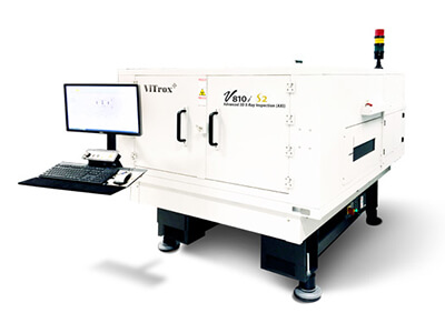
1-Complete solution for large boards
2- Stronger defect verification test results
3-M2M link function of smart factory through V-ONE
4- Get well-known CM and OEM strong recommendation
5-X-ray online detection of PCBA widely used in automotive electronics, server motherboards, medical electronics, aerospace, etc.
| Allowable Panel Characteristics | V810i S2EX | V810i S2 XXL | V810i S2 XLT |
|---|---|---|---|
| PCB maximum size | 482 mm x 610 mm (19"x24") | 660 mm x 965 mm (26"x38") | 660 mm x 965 mm (26"x38") |
| PCB minimum size | 76 mm x 76 mm (3" x 3" ) | 76 mm x 76 mm (3" x 3" ) | 76 mm x 76 mm (3" x 3" ) |
| Maximum measurable board width | 474 mm x 610 mm (18.7"x24") | 654 mm x 965 mm (25.75"x38") | 654 mm x 965 mm (25.75"x38") |
| Maximum thickness | 7 mm (276 mils) | 12.7 mm (500 mils) | 12.7 mm (500 mils) |
| Minimum thickness | 0.5 mm (20 mils) | 0.5 mm (20 mils) | 0.5 mm (20 mils) |
| Plate bend | Downside < 3.3 mm; Upside < 1.5 mm | Downside < 3.3 mm; Upside < 3.3 mm | Downside < 3.3 mm; Upside < 3.3 mm |
| Maximum plate weight | 4.5kg | 15kg | 15kg |
| 50 mm @ 23 µm resolution | 25 mm @ 19 µm resolution | 50 mm @ 19 µm resolution | |
| 38 mm @ 19 µm resolution | 15 mm @ 13 µm resolution | 31 mm @ 15 µm resolution | |
| Upper resolution | 38 mm @ 10.5 µm# resolution | * Calculated from Board Top surface | 13 mm @ 11 µm resolution |
| 11 mm @ 11 µm resolution | 31 mm @ 10 µm resolution | ||
| 11 mm @ 6 µm# resolution | 13 mm @ 7.5 µm resolution | ||
| * Calculated from Board Top surface | * Calculated from Board Top surface | ||
| Lower gap | 70 mm | 80 mm | 80 mm |
| Edge clearance | 3 mm | 3 mm | 3 mm |
| Board width error | ±0.7 mm | ±0.7 mm | ±0.7 mm |
| System resolution | 23 µm/19 µm#, 11 µm, 10.5µm, 6µm# | 19 µm/13 µm | 19 µm/15 µm /11 µm/10µm/7.5 µm |
| 100% press test capability | Yes (With PSP2 feature) | Yes (With PSP2 feature) | Yes (With PSP2 feature) |
| Can withstand PCB temperature | 40 ℃ | 40 ℃ | 40 ℃ |
| Power and Environmental | |||
| width * deep * high | 1566 mm x 2145 mm x 1972 mm | 2240 mm x 2460 mm x 1980 mm | 2240 mm x 2460 mm x 1980 mm |
| weight | ~3500 kg | ~5500 kg | ~6000 kg |


